SPM-TH
Scanning Probe Microscopy Theory & Nanomechanics GroupForces and Transport in Nanostructures
Research Highlights
It is possible to "write" with atoms using an Atomic Force Microscope
Nanotechnology exploits the properties of materials on a nanometric scale, (a nanometer is one millionth of a millimeter). The ultimate limit for such miniaturization is the development of devices formed by atomic structures created artificially to fulfil a determined purpose. The tools that permit the visualization and manipulation of atoms are called Scanning Probe Microscopes. This includes the Scanning Tunneling Microscope (STM), whose development earned G. Binning and H. Rohrer the Nobel prize for physics in 1986, and more recently the Atomic Force Microscope (AFM). In a study published in Science magazine, an international team of scientists, including researchers from the Theoretical Condensed Matter Physics department at the Universidad Autónoma de Madrid, present a new method for the manipulation of atoms based on the AFM that makes it possible to build stable atomic structures at room temperature.
Unlike all previously developed atomic manipulation methods that consist of pushing or pulling atoms from the surface of a material using the tip of the microscope and require very low temperatures, the new method is based on the controlled interchange of an atom at the tip for a surface atom when the two are close enough. Using the atoms at the tip (that are chemically different to those at the surface) as "ink", it is possible to "write" or "draw" with the microscope. This interchange process can be repeated in different positions over the surface to form complex structures very efficiently. In particular, this group has "written" the chemical symbol for silicon "Si" (which is the chemical element used as "ink") on a surface covered with tin atoms. Thanks to numerical simulations based on quantum mechanics that require the use of supercomputers it has also been possible to explain the basic atomic mechanism behind this process and determine the conditions under which it takes place.
This new manipulation scheme drastically reduces the time necessary to realize complex atomic structures. It can even be used at room temperature and has been proven to work on various semiconductor surfaces. Therefore, this method opens new perspectives in fields like Material Science, Nanotechnology, Molecular Electronics and Spintronics. In particular, the combination of the capacity of the AFM to manipulate individual atoms on surfaces with the possibility of identifying the chemical element. This was demonstrated by the same team in an article published in last year's Nature and will enable the construction of nanostructures with properties and functionalities specified to improve the yield of electronic devices. For example, placing specific dopant elements in the best position on semi-conductive surfaces to increase the efficiency of nanometric transistors or magnetic atoms would open the possibility of developing devices based on the control of the spin of an electron. These techniques could also bring the possibility of "nano-facturing" of qbits, which are the basic components of what could eventually become a quantum computer.
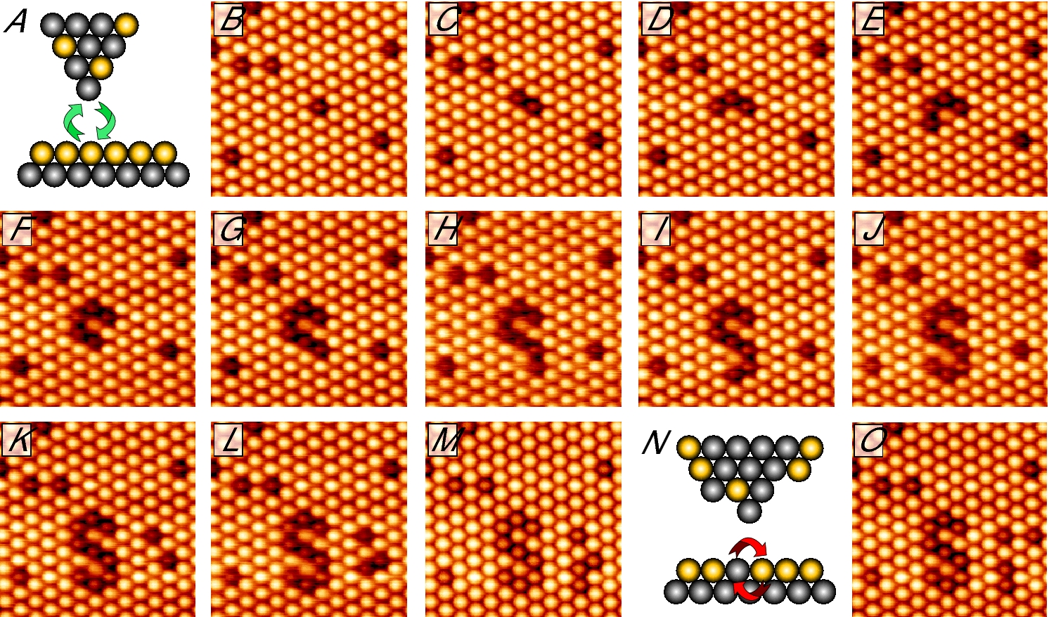
Fig. 1 Creation of atomic patterns displaying the symbol of silicon by vertical interchange atom manipulation at room temperature. These experiments have been performed on a Si surface covered by a single layer of Sn atoms (bright "points" in the image), that naturally includes some Si atoms (dark "points") as substitutional defects. Approaching the tip to the surface we can induce the interchange of a Si atom from the tip (the "ink") with a Sn atom from the surface. Complex patterns can be constructed by the successive repetition of this process. The last step is a lateral in-plane manipulation where a surface Sn atom is interchanged with the neighbouring Si defect.
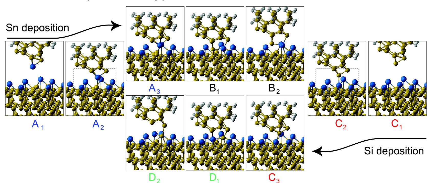
Fig. 2 First-principles simulations of the vertical interchange atom manipulation proceses (yellow balls correspond to Si atoms and blue ones to Sn atoms). The key of the interchange process is the formation of a dimer structure with the last tip atom and the surface atom (B1 y D1). In this structure both atoms have the same number of bonds with the neighbouring atoms and have lost their preferential association with the tip or the surface. Upon tip retraction, the interchange process takes place, leaving on the surface the atom that was originally at the tip apex. These simulations are based on quantum mechanics and require the use of large supercomputers.
Yoshiaki Sugimoto 1, Pablo Pou 2, Oscar Custance 3, Pavel Jelinek 4, Masayuki Abe 1, Rubén Pérez 2 & Seizo Morita 1.
Complex patterning by vertical interchange atom manipulation using atomic force microscopy
Science 322 , 413-417 (2008).
(DOI link)
(pdf)
1 Graduate School of Engineering, Osaka University, 2-1 Yamada-Oka, 565-0871 Suita, Osaka, Japan.
2 Departamento de Física Teórica de la Materia Condensada, Universidad Autónoma de Madrid, 28049 Madrid, Spain.
3 National Institute for Materials Science, 1-2-1 Sengen, 305-0047 Tsukuba, Ibaraki, Japan.
4 Institute of Physics, Academy of Sciences of the Czech Republic, Cukrovarnicka 10, 1862 53, Prague, Czech Republic.
