SPM-TH
Scanning Probe Microscopy Theory & Nanomechanics GroupForces and Transport in Nanostructures
Research Activities
Theory of Scanning Tunneling (STM) and Atomic Force (AFM) Microscopes
Semiconductor surfaces, well characterized by many different surface science techniques, are the perfect playground to develop new Scanning Probe Microscopy (SPM) techniques. Surface reconstructions, like the famous Si(111)-7x7, have become prototypical tests to determine the limits on accuracy and applicability of STM/AFM microscopies. Our long–standing theoretical work in these surfaces, in collaboration with experimental groups, has pushed the boundaries of Frequency Modulation (FM) AFM, usually known as Non-contact AFM, showing its ability for imaging, chemical identification and manipulation at the atomic scale.
Electronic transport on C60/metal nanostructures surface
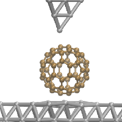 |
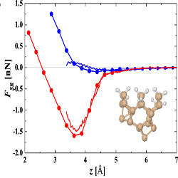
Over the last 15 years, we have developed an ab initio approach, STMAD, to compute the transport properties of nanostructures. The method combines DFT calculations on a local orbital basis with Non- equilibrium Green’s Functions (NEGF). Applications of this methodology span a wide variety of problems ranging from the conductance of metallic nanowires to the simulation of STM images including explicitly the STM tip [1, 2] . We are currently improving STMAD to take advantage of the flexibility and accuracy offered by large basis sets (as in OpenMx or SIESTA) and to handle efficiently very large and complex systems, like C60 adsorbed on metal and oxide surfaces. Project members: C. Romero, L. Zotti, R. Pérez.External collaboration: J. A. Martín-Gago (ICMM-CSIC, Madrid). |
Exploring the ultimate STM/AFM capabilities: Creating a Si tetramer on the Si (111)7x7 surface
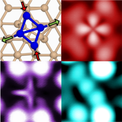 |
This project combines experiments and theory to understand the puzzling STM and FM-AFM images obtained on a Si tetramer, an artificial molecule built by atomic manipulation with the FM-AFM on the Si(111)-7x7 surface. DFT calculations show that the system is bi-stable, with two solutions characterized by a rhombohedral tetramer with one of the Si atoms protruding over the other three. Thermal energy and/or large bias can activate the switching between these two asymmetric structures leading to a symmetric STM image. In the case of FM-AFM, the situation is even more complex as the tip-surface interaction also plays an important role. Project members: L. Rodrigo, P. Pou, R. PérezExternal collaboration: Y. Shiro, M. Abe, Y. Sugimoto and S. Morita (Osaka University, Japan); P. Mutombo, P. Jelínek (FZU, Prague, Czech Republic) |
Observation of Quantum Degeneracy based on the relation between force and current simultaneously measured by RT STM/AFM experiments
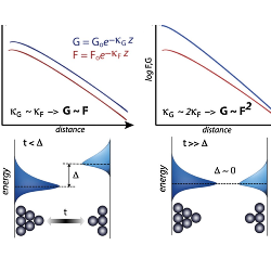 |
Quantum degeneracy is a key concept in quantum mechanics with large implications to many processes in condensed matter. The strongly localized dangling-bond states at the Fermi level in the Si(111) 7x7 reconstruction [1], provide a unique test bed to unravel the consequences of electron energy level degeneracy on the tunneling conductance, G, and the chemical force, F, at the atomic scale. G and F decay exponentially with distance, usually maintaining a direct proportionality G / F. However, we show that a square relation G / F2 arises as a consequence of quantum degeneracy between the interacting frontier states of the scanning tip and a surface atom [2] . Project members: P. Pou, R. PérezExternal collaboration: Y. Sugimoto, M. Abe, and S. Morita (Osaka University, Japan); M. Ondracek, P. Jelínek (FZU, Prague, Czech Republic); F. Flores (UAM, Madrid) |
Atom Manipulation with FM-AFM: Role of the Tip Chemical Reactivity
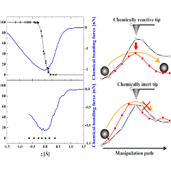 |
Early experiments of atom manipulation were performed with weakly interacting adsorbates on metal surfaces at low temperature. Adatoms on semiconductor reconstructions are covalently bonded (~1 eV), offering the possibility to study manipulation at room temperature. In a previous project, we have shown the feasibility of the process and unraveled the complex atomistic mechanisms involved [1, 2] . Here, we rationalize measurements of the atom-hopping probabilities associated with different manipulation processes on the Si(111)-7x7. We show that the ability to reduce the energy barrier that controls the Si adatom movement towards a vacancy site correlates with the tip chemical reactivity, reflected in the maximal attractive force [3] . Project members: P. Pou, R. PérezExternal collaboration: Y. Sugimoto, A. Yurtsever, M. Abe, and S. Morita (Osaka University, Japan); M. Ondracek, P. Jelínek (FZU, Prague, Czech Republic) |
Force mapping on partially covered H-Si(111) 7x7 surface: Force vs site/tip reactivity
 |
The combination of force spectroscopy and theoretical calculations is a really powerful tool to understand the contrast mechanisms in FM-AFM. This methodology provided the basis for our demonstration of chemical identification of individual surface atoms [1] . Here we use force mapping experiments on the H- Si(111)-(7x7) surface (exposing both reactive Si adatoms and H-passivated sites), supported by our DFT simulations, to identify two types of tip termination with very different interaction strengths: a dimer- terminated Si tip, yielding the common strong covalent interaction, and an OH-terminated Si tip, featuring a weak electrostatic interaction, that is responsible for the weak image contrast [2] . Project members: P. Pou, R. PérezExternal collaboration: A. Yurtsever, Y. Sugimoto, M. Abe, and S. Morita (Osaka University, Japan); M. Ondracek, P. Jelínek (FZU, Prague, Czech Republic) |
