SPM-TH
Scanning Probe Microscopy Theory & Nanomechanics GroupForces and Transport in Nanostructures
Research Activities
Graphene and carbon nanostructures
The 2D nature of graphene makes SPM techniques the optimal tools to characterize its local electronic and mechanical properties at the atomic scale. We combine SPM experiments and our atomistic simulations using both DFT and classical approaches to study these materials under realistic operating conditions, where we take into account how the “environment” --the coupling with the substrate underneath and the presence of defects and contaminants-- locally modifies graphene native properties. Understanding these local modifications would allow the tuning of the properties of these 2D materials in order to integrate them efficiently in future real nanodevices.
Electronic and Mechanical properties of defective graphene
 |
Magnetic order in graphene and graphene-based materials relies on the formation of magnetic moments and a sufficiently strong mutual interaction. Vacancies are considered the primary source of magnetic moments. Theoretical publications so far deal with the case of a single vacancy in rather small cells. In this project we have gone a step further calculating in larger supercells and also with realistic defect concentrations. We have also extended our work to the mechanical properties of defected graphene performing both quantum and classical calculations. Our goal is to characterize the changes in Young’s modulus, flexibility and failure modes compared to the ideal case. Project members: L. Rodrigo, P. Pou, M. Ortega, G. Vilhena, R.PérezExternal collaboration: G. López-Polin, C. Gómez-Navarro, J. Gómez-Herrero (UAM) |
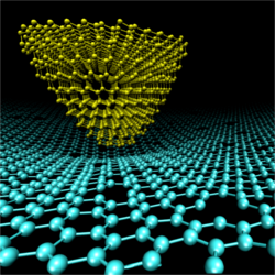
Resolving the Moire patterns with AFM on Gr/Pt
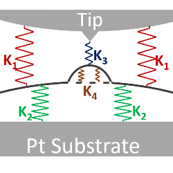 |
Atomic resolution –including a contrast inversion from honeycomb to hexagonal-- and moiré patterns have been observed with AFM on Gr/Pt(111). Our DFT calculations link the contrast inversion with the electronic density dependence of the Pauli interaction. Corrugated moirés can be explained by DFT in the repulsive regime, where the tip indents the graphene sheet deep enough so the displaced carbon atoms act as a tip that allows sensing the Pt surface with atomic resolution. This subsurface resolution may be generalized to other 2D materials. Understanding the Moires in the attractive regime and the observed dissipation requires a model that takes into account the global and local elastic response of the graphene. Project members: M. Ellner, P. Pou, R. PérezExternal collaboration: B. de la Torre, N. Nicoara, J. M. Gómez-Rodríguez |
Graphene growth on metal steps
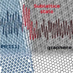 |
This project combines high resolution RT-STM experiments with DFT calculations and STM simulations to unveil the atomic structure of a border-like edge between a Pt(111) step and a graphene zigzag edge [1]. The graphene edges minimize their strain by inducing a 3-fold edge-reconstruction on the metal side. The G-edge state is shifted to +0.8 eV above Fermi level, highly localized in one of the graphene sublattices and confined to the G-Pt interface. This state spreads out inside the first Pt row resulting in a high quality G-metal electric contact that could be relevant for designing future atomically precise graphene metal leads. Project members: L. Rodrigo, P. Pou, R. Pérez.External collaboration: P. Merino , A. L. Pinardi, J. Méndez, M. F. López, J. A. Martíxn-Gago (CAB-INTA & ICMM-CSIC) |
Graphene grown over transition metal substrates: Defects & Moire patterns
 |
Understanding the coupling of graphene with its local environment is critical to integrate it in tomorrow's electronic devices. Highly perfect sheets of graphene can be obtained by epitaxial growth on metal surfaces, and for some transition elements, like Cu or Pt, the interaction is so weak that many characteristic properties of graphene are preserved. We have already shown the effect that a Pt substrate has on the structural and magnetic properties of a tailored (with single C vacancies) graphene layer [1], and we are currently studying the structural and electronic characteristics of graphene on Cu(111) using DFT (including van der Waals dispersion) and STM/STS experiments. Project members: D. Fernández-Torre, C. Romero, P. Pou, R. Pérez.External collaboration: M. Moreno-Ugeda, A. J. Martínez-Galera, A. Recio, J. M. Gómez-Rodríguez & H. González-Herrero, I. Brihuega (UAM) |
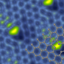
Understanding the AFM/STM contrast in carbon nanostructures
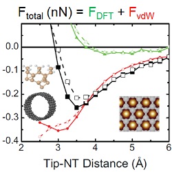 |
First-principles calculations show that the rich variety of image patterns found in carbon nanostructures with AFM and STM can be rationalized in terms of the chemical reactivity of the tip and the distance range explored in the experiments [1]. For weakly reactive tips, the Pauli repulsion dominates the atomic contrast and force maxima are expected on low electronic density positions as the hollow site. With reactive tips, the interaction is strong enough to change locally the hybridization of the carbon atoms, making it possible to observe atomic resolution in both the attractive and the repulsive regime although with inverted contrast. Regarding STM images, we show that in the near-contact regime, due to current saturation, bright spots correspond to hollow positions instead of atomic sites, providing an explanation for the most common hexagonal pattern found in the experiments. Project members: P. Pou, R. Pérez.External collaboration: M. Ondracek, P. Jelínek (FZU, Prague, Czech Republic) |
